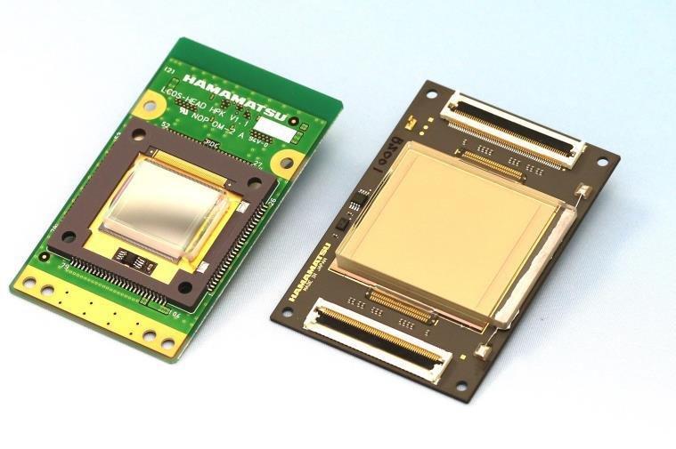
Hamamatsu Photonics has developed a new spatial light modulator (SLM) with the world’s largest-class effective area and vastly improved heat resistance
A portion of this R&D was a commissioned project entitled "Photonics and Quantum Technology for Society 5.0". Known as a second term project of the Cross-ministerial Strategic Innovation Creation Program (SIP), it is sponsored by the Japanese Cabinet Office Council for Science, Technology and Innovation, and managed by the National Institutes for Quantum and Radiological Science and Technology (QST).
*1: A spatial light modulator or SLM is an optical device that utilizes a liquid crystal to control the wavefront of incident light from lasers for example and adjust the wavefront shape of the reflected light. Using a SLM allows to freely control the laser beam pattern to branch the incident light and correct its distortion for example
Product overview
Lasers are broadly classified as pulsed lasers that repeatedly emit light pulses at short time intervals and as CW lasers that emit a continuous light beam. While pulsed lasers are capable of high-precision laser processing and machining with minimal heat damage, CW lasers are the mainstream of laser machining since these can be used to heat and treat metallic materials by laser welding and cutting, etc.
Using our unique thin-film and integrated circuit design technology, we have succeeded in creating a SLM with the world’s highest resistance to light for industrial pulsed laser systems. This SLM can spread a high-power pulsed laser’s output into multiple beams for the multi-point processing of hard-to-machine materials such as carbon-fiber-reinforced polymers (CFRP). This feature ensures higher speed and higher accuracy compared to focusing the laser beam onto a single point. This SLM can also be used with CW laser systems but has a problem that its performance tends to degrade due to a temperature rise in the SLM.
The SLM has a liquid crystal layer sandwiched between a silicon substrate with pixel electrodes and a glass substrate with a transparent electrode. The path length of the incident light is controlled by the inclination or tilt of each liquid crystal via the pixel electrodes, and the reflected light. Modulation in order to freely control the laser irradiation pattern is done in this way and can be used for example to split the incident light or correct its distortion.
By applying stitching techniques, *2 instigated when we were developing and manufacturing large-area opto-semiconductors, we built the new SLM with an effective area of 30.24 mm × 30.7 mm, about 4 times larger than our previous one. This is one of the world’s largest currently available liquid-crystal SLM and it effectively reduces the incident energy per unit area on the SLM. This new SLM also employs a large ceramic substrate with excellent heat resistance and thermal conductivity to improve heat dissipation efficiency. It successfully suppresses the temperature rise occurring during irradiation with a CW laser, making this SLM ideal for high-power industrial CW laser systems. Usually, large area silicon substrates are prone to warping and deterioration in flatness during the manufacturing process which distorts the irradiation beam patterns and shapes. However, using our unique opto-semiconductor manufacturing technology, we also developed a technique that maintains the substrate flatness while increasing the SLM effective area. This provides a beam shape controllable to a high degree of accuracy.
Using this new SLM in an industrial CW laser system for multi-point simultaneous processing will improve laser thermal processing efficiency in laser welding and laser cutting tasks as well as metal 3D printing. Moreover, accurately controlling and optimizing the beam shape according to the material and shape of the object will provide even higher precision in laser thermal processing.
We are working to optimize the dielectric multilayer film mirror that makes up this newly developed SLM to further improve its resistance to light. We will also push ahead with demonstration tests using laser processing machines equipped with our SLM.
*2: Stitching technique is a method for repeatedly exposing semiconductor circuits to a silicon substrate. This allows fabricating large circuit patterns that cannot be entirely exposed all at once.
Development background
SIP’s second term projects intend to demonstrate innovative manufacturing and fabrication through a cyber-physical system (CPS) that merges cyberspace (virtual space) and physical space (real space) to a high degree. Among these projects, the “Photonics and Quantum Technology for Society 5.0” project has R&D themes in three areas including laser processing and aims to demonstrate innovative manufacturing and fabrication with a CPS-type laser processing system.
If CPS-type laser processing systems are developed, these could optimize design and manufacturing processes by accumulating the processing data obtained by irradiating an object with a laser under many different conditions and then selecting the optimal processing conditions using artificial intelligence (AI). To this end, we have been working to improve the performance of SLMs, which are essential devices for CPS-type laser processing systems.
Hamamatsu Photonics Deutschland GmbH
Arzberger Str. 10
82211 Herrsching am Ammersee
Telefon: +49 (8152) 375-0
Telefax: +49 (8152) 375-199
http://www.hamamatsu.com
Public Relations
Telefon: +49 (8152) 375-185
Fax: +49 (8152) 375-199
E-Mail: rfritsch@hamamatsu.de
![]()

Das könnte dich ebenfalls interessieren
Spektrometer M522 jetzt mit drei Ausgangsports
robogonio – multifunktionaler am Start