Microphotonics meets microelectronics: Atomic layer processing for silicon carbide-based quantum photonic circuits
Quantum systems are the rising stars of future technologies. Large high-tech companies, and institutional investors in particular, are engaged in a global race to transfer the phenomena of quantum mechanics from research laboratories into broader practical applications. Revolutions are already taking place in information processing, sensor technology and communication that will permanently transform entire economic sectors and societies.
From a technological perspective, quantum systems are best described as a combination of quantum physics, photonics and electronics. The quantum computer is undoubtedly the most popular example of this. Current quantum systems still resemble complicated optoelectronic laboratory setups to a large extent, and immense technical effort is required to generate, manipulate and process quantum states. Complexity and sheer size are limiting factors, and the cooling required is an issue, as many of the currently available solutions only work at temperatures close to absolute zero.
Integrating quantum technologies into marketable products and services therefore requires considerable research and development efforts to create essential basic technologies. Similarly, the economic realisation of practical quantum systems lacks a uniform, future-proof material platform that would enable significant advances in miniaturisation, enhanced performance, and reduced costs.
Robust, connectable, quantum-compatible: silicon carbide as a key quantum material
Due to its unique physical properties, the semiconductor material silicon carbide (SiC) is a promising technology platform for solid-state quantum systems. SiC is a wide bandgap (WBG) semiconductor and has become established in recent years, particularly in the field of power electronics. It is also highly attractive for developing photonic microsystems and photonic integrated circuits (PICs) because it can be used to manufacture optical devices, light sources, and sensors. Furthermore, SiC is of interest due to nonlinear optical effects that can be exploited to modify the colour of laser light. For instance, it can be used to convert infrared light into visible light very efficiently. The possibility of integrating point defects in the form of color centers that function at room temperature means SiC may even allow the direct integration of quantum functionality in the future. “This makes silicon carbide an ideal platform for photonics, electronics, and quantum applications,” explains Dr. Pascal Del’Haye, who heads the project at the Max Planck Institute for the Science of Light.
SiC could therefore be used to produce all the elements required for the construction of powerful, miniaturised quantum systems. It is compatible with microelectronics and microphotonics, and offers new quantum electronic functions. Since it is compatible with the easily controllable CMOS processes of classic silicon technology, SiC would be ideal for the industrial mass production of quantum PICs.
Optimization of the first microphotonic devices paves the way for SiC quantum chips
There is still a long way to go before optoelectronic quantum chips become a reality, and research in this area is still more or less in its infancy. To build PICs, standardized microphotonics devices with minimal optical losses are needed. Optical waveguides and ring resonators that can efficiently guide or store light in tiny structures are essential for this. While waveguides perform the function of loss-free optical lines, resonators consist of tiny rings in which the input light completes up to a million cycles. The photon storage times achieved in this way allow these devices to be charged with high circulating optical power, enabling a variety of nonlinear optical effects. For example, micro-resonators can convert laser light of a specific wavelength into an optical frequency comb, i.e., a light source consisting of several discrete frequencies, which can be used, for example, for very fast parallel data transmission in telecommunications networks.
Another useful effect is the interaction of counter-propagating light. The nonlinear optical coupling of counter-propagating light in ring resonators leads to spontaneous symmetry breaking that allows light to circulate in only one direction, i.e., clockwise or counterclockwise. This can be used, for example, to implement chip-integrated optical diodes, photonic switches, or optical sensors, which enable the construction of more complex photonic systems.
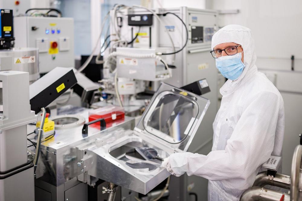
However, the quality of the photonic devices manufactured on SiC substrates is not yet optimal, and the relatively high surface roughness causes optical losses in the waveguides and resonators. Flawless surfaces are essential to ensure that photons can move quickly and do not tunnel outwards. A promising solution is to smooth the component surfaces using atomic layer etching (ALE) to create well-defined interfaces and minimize loss and scattering centers.
Bridging the gap between basic research and process development in the ALP-4-SiC project
In order to develop a novel manufacturing process for complex photonic devices based on silicon carbide, basic and application-oriented research must collaborate intensively. In the ALP-4-SiC project – atomic layer processing for SiC for applications in photonics and quantum communication – MPL in Erlangen and the Fraunhofer IISB with its Fraunhofer Technology Center for High-Performance Materials THM in Freiberg are pooling their expertise. MPL has extensive experience in the design and characterization of photonic components, while the IISB contributes its expertise in the field of SiC semiconductor technology and atomic layer processing.
The new approach of integrating atom layer-based processes for photonic devices with significantly improved optical properties has great potential for the future commercialization of integrated photonic devices. In the medium term, manufacturers of ALE process equipment in particular could tap into new customer groups and, in return, position photonics suppliers with innovative products in a rapidly growing market. However, the long-term effects of the availability of a universal, practical, scalable technology platform for integrated quantum optoelectronic circuits based on SiC cannot be predicted at this stage.
Max Planck Institute for the Science of Light (MPL)
The Max Planck Institute for the Science of Light (MPL) covers a broad spectrum of research, including non-linear optics, quantum optics, nanophotonics, photonic crystal fibers, optomechanics, quantum technologies, biophysics, and—in collaboration with the Max-Planck-Zentrum für Physik und Medizin—links between physics and medicine. MPL was founded in January 2009 and is one of more than 80 institutes of the Max Planck Society that conduct basic research in the natural sciences, life sciences, humanities, and social sciences for the benefit of society.
Fraunhofer Technology Center for High Performance Materials THM
The Fraunhofer Technology Center for High Performance Materials THM in Freiberg, Saxony, is a research and transfer platform of the Fraunhofer Institute for Integrated Systems and Device Technology IISB and the Fraunhofer Institute for Ceramic Technologies and Systems IKTS. Together, semiconductor and energy materials are being transferred to new applications, with particular emphasis on material recycling. The activities at Fraunhofer THM are focused on the analysis and development of sustainable battery systems with improved life cycle assessment and raw material availability as well as the research and evaluation of innovative semiconductor components and the associated process steps.
Funding information
The ALP-4-SiC project – atomic layer processing for SiC for applications in photonics and quantum communication – is funded as part of the “Scientific Preliminary Projects (WiVoPro, Quantum Technologies in Germany)” program of the German Federal Ministry of Research, Technology and Space (BMFTR). The projects funded by the BMFTR with this measure investigate scientific issues with a view to future industrial applications. They can be carried out by up to two research institutions and are intended to bridge the gap between basic research and industry-led joint funding.
The Fraunhofer Institute for Integrated Systems and Device Technology IISB is one of Europe’s leading research institutions for wide-bandgap semiconductors and power electronics, covering the complete value chain. The spectrum ranges from basic materials, semiconductor devices and process technologies, power electronic modules and components to complex power electronic and energy systems.
Main target applications of the IISB are semiconductor manufacturing, electromobility, aerospace, sustainable energy supply as well as civil security. With its solutions, the institute has been setting benchmarks in energy efficiency and performance, even for extreme operating conditions. The integration of intelligent data-based functionalities also continuously opens up new application scenarios. This allows the IISB to support customers and partners worldwide in transferring scientific results into commercial products.
A total of around 400 employees work at the IISB’s locations: the headquarters in Erlangen, the Cleantech Innovation Park in Hallstadt, and the Fraunhofer Technology Center High Performance Materials THM in Freiberg.
Fraunhofer-Institut für Integrierte Systeme und Bauelementetechnologie IISB
Schottkystraße 10
91058 Erlangen
Telefon: +49 (9131) 761-0
Telefax: +49 (9131) 761-390
http://www.iisb.fraunhofer.de
Group Manager Spectroscopy and Test Devices
Telefon: +49 3731 2033-103
E-Mail: franziska.beyer@iisb.fraunhofer.de
![]()


Das könnte dich ebenfalls interessieren
Die Ellbogen ausfahren gegen Corona
Simulationen in der Prozessoptimierung