VON ARDENNE Launches New OPTA X300 Deposition Tool and Opens New Cleanrooms in Dresden, Germany
“As the semiconductor industry pushes the boundaries of performance and miniaturization, VON ARDENNE is stepping into the US market with next-generation tool platforms, co-developed materials solutions, and custom refurbishment and upgrade services,” said Guido Ueberreiter, vice president of semiconductor strategy at VON ARDENNE. “Our approach enables semiconductor manufacturers to overcome complex deposition and vacuum challenges, particularly where legacy tools fall short or off-the-shelf solutions can’t meet emerging needs. Our OPTA X300 platform is purpose-built for high precision double-sided deposition to support the most demanding multilayer applications.”
Flagship Showcase: OPTA X300
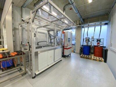
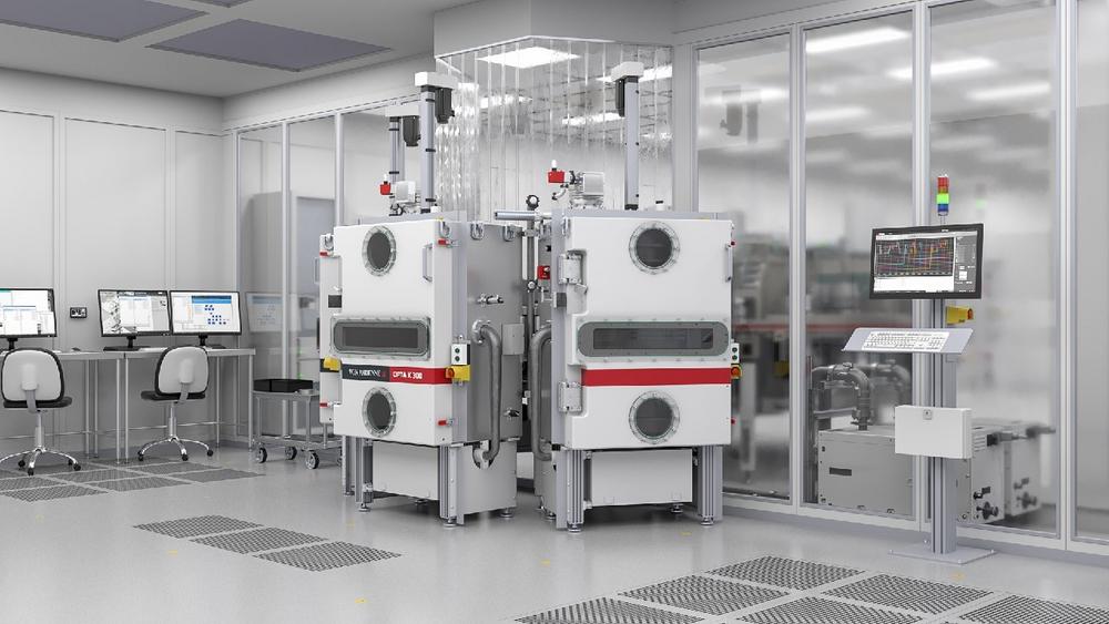
At SEMICON West, VON ARDENNE will feature its OPTA X300 rotary disk coating system, the company’s flagship platform for sub-nanometer precision deposition on demanding substrates. Purpose-built for electrical and optical layers for memory, photonics and sensor devices, the OTPA X300 offers flexibility to support customers from R&D through high-volume manufacturing.
The OPTA X300 platform will be installed at VON ARDENNE’s new ISO 5 cleanroom in Dresden, which serves as a cornerstone of its Technology and Applications Center. This facility enables customers to test, sample and co-develop deposition processes with access to industry-leading engineering and materials science expertise.
Cleanroom Capabilities
The new cleanroom features 200 m2 of ISO 5 (Class 100) assembly and test bays with airborne molecular contamination control (AMC) as well as 400 m2 of ISO 7 cleanroom manufacturing space in Dresden. The cleanroom is designed for semiconductor, optical and space applications and is extreme ultraviolet (EUV)-ready. The OPTA X300 will be available for customer demos and co-development projects starting mid-2026.
“US fabs need more than tool suppliers, they need engineering partners who understand both the equipment and the materials science behind next-generation devices,” said Michael Schneider, vice president of semiconductor and precision optics at VON ARDENNE. “We’re bringing that integrated expertise to the US market—helping customers unlock new levels of performance, customization and yield.”
Also being showcased at the VON ARDENNE SEMICON West booth are its HISS600, designed to deliver superior uniformity and high throughput for panel-level packaging, and VISS, a modular vertical coating platform ideal for scaling from lab to production for substrates up to 600 mm.
For more information, visit https://vonardenne.us/industries-applications/semiconductors/. To schedule a demo or speak with a VON ARDENNE representative, contact radach.daniel@vonardenne.com.
VON ARDENNE combines high-precision engineering and unmatched depth in materials science expertise to deliver advanced deposition and vacuum system solutions with configure-to-order flexibility and sub-nanometer precision for all substrate sizes and materials.
With deep scientific expertise, flexible tool platforms, and a collaborative approach, VON ARDENNE empowers semiconductor customers to scale from R&D to high-volume manufacturing and solve advanced coating challenges that conventional vendors can’t touch. For more information, visit https://vonardenne.us/.
VON ARDENNE GmbH
Am Hahnweg 8
01328 Dresden
Telefon: +49 (351) 2637-300
Telefax: +49 (351) 2637-308
http://www.vonardenne.de
Marketing und Kommunikation
Telefon: +49 351 2637-300
E-Mail: iser.falk@vonardenne.com
![]()